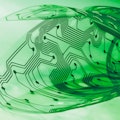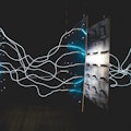
Electronics
Guilherme Henrique @ Envisioning
It could be said that electronics, which dates back to 1745 with the invention of the Leyden jar, is the science and technology devoted to harnessing electricity. All matter has electrical properties and electricity is an essential ingredient of it. History has plenty of gadgets that generate, store, control and switch the traveling of electrons through conductive materials, as silver, gold, iron, copper — bringing forth at the end of the day an electrical current for a particular purpose. But the flow can also devoid of matter. In any case, without electronics nothing would move in this world but animals and organic matters.
Along the path that goes from static electricity to solid-state electronics, one encounters a colossal amount of methods and applications. In the light of all this, and without being simplistic, we must remain within the confines of Goldilocks, working toward the middle ground of integrated circuits. We strongly recommend to beginners the reading of Forrest M. Mims, III's Getting Started in Electronics, a book designed to look as though it were a binder containing pages hand-lettered with simple elegance.
E-skin Patches
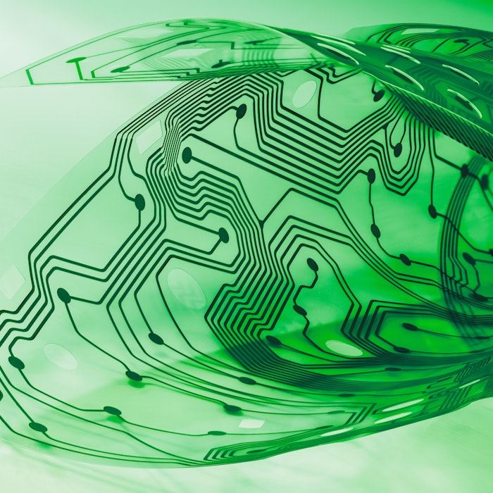
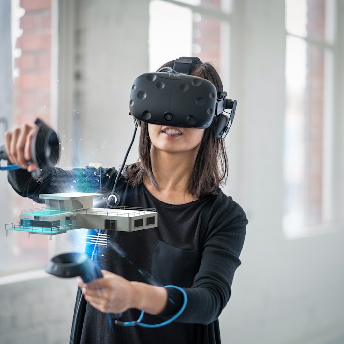
When it comes to wearable technologies, electronic devices often sound the most commonplace to start with. But if you are going to incorporate an accessory into the body, you had better off wear something malleable, something more comfortable and ergonomic. Thus far, in the conducting of tests with alternative substrates, results fall short of connecting soft conductors with rigid electronic components, as LED displays. There is one plot twist, however, as recent research obtained significant results in the so-called stretchable electronics, or thin circuit assemblies made from Eutectic Gallium–Indium, a material capable of keeping liquid forms at room temperature.
This breakthrough paves the way for the consolidation of electronic skin, flexible electronic devices, or stretchable circuits that can be 'patched' onto the skin to act as sensing prosthesis. They are made of piezoelectric polymers, as to say, they can generate electrical voltage in response to mechanical pressure of body movement. Batteries not required. Self-quantification will never be the same...
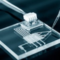
Wooden Chips and Bio-inks
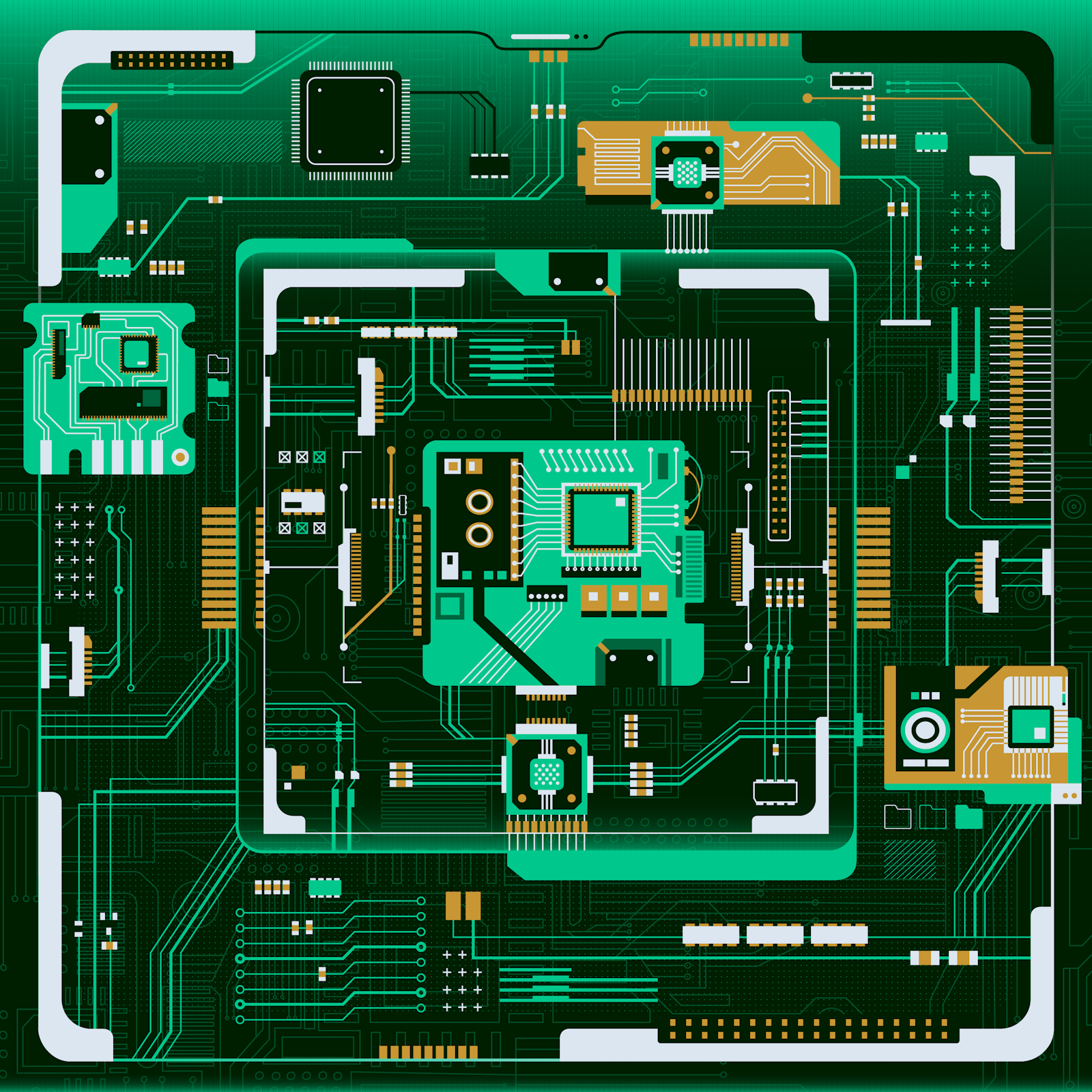
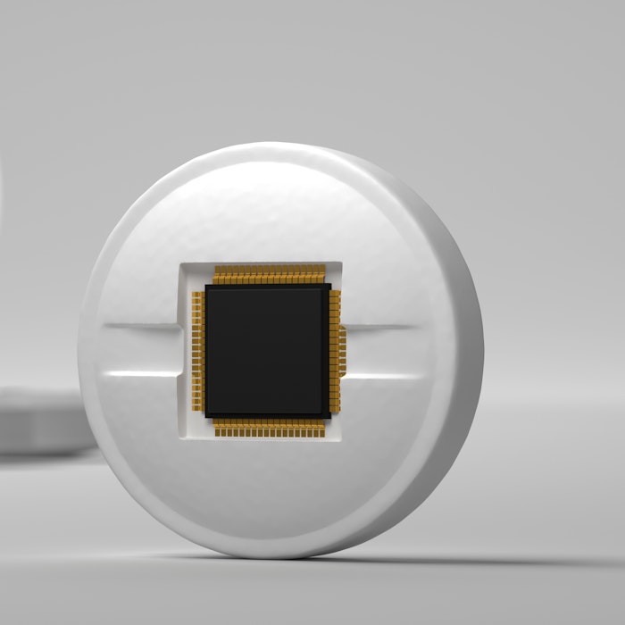
There is a train of thought in which electronics can be summed up to microchips and silicon, the most widely used semiconductor material in computer integrated circuits. Chips and silicon were thus meant to epitomize the domain. But thoughts can do better. And the more the mind opens up the better. Beginning with biodegradable semiconductor chips made out of wood. Just release etched circuits from original substrates ―usually aluminum― and 'tattoo' them onto a nanofibril biopolymer. Voila, you have a wood chip. This makes a lot of sense in a world where the e-waste growth recorded annually is around 2.5 million metric tonnes.
In the corporate world, DuPont has moved to thinking about mold electronics, or how the American company refers to "printed electronic circuitry on a polymer film substrate which successively undergoes a thermoforming". Its efforts are currently focused on the improvement of conductive ink and 'intelligent surfaces' for the automotive interiors segment. It is fed up with flat and rigid constraining of the hitherto design options. And it might be part of a pattern. As it could not be otherwise, photovoltaic cell manufacturers are also eyeing this technology, but with an eco-friendly look. Rather than having a palette of well-known elements, as silver, imagine we had a conductive surface printed with a 'bio-ink' of cyanobacteria, creating a biophotovoltaic cell. It may sound like balderdash, but it works.
What Lies Ahead
Molecular electronics
It is still in the early trials of laboratory tests, rivaling nanotechnology's honorable vision to save Moore's law from miniaturization limits. Such electronics tamper with molecular building blocks in order to build hydrocarbon chains, the so-called 'molecular wires', for microcircuits. Those functions certainly as conductors, but also as molecular switches and transducers of information signals. Two-dimensional semiconductor is the one most awaited application, a graphene thin-layered structure not susceptible to loss of coherence, the Achilles heel of quantum computing.
'Molar' electronics
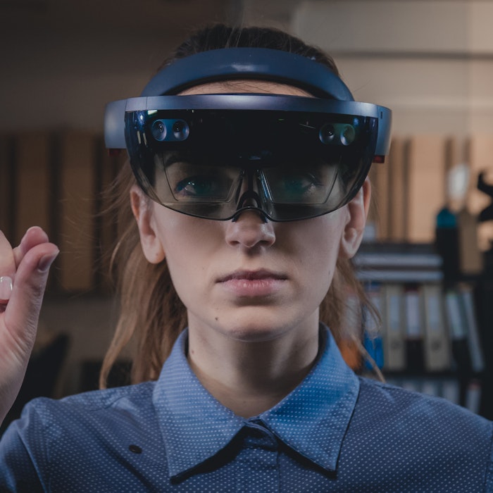
Going a dimension further, certainly organic electronics, a discipline that studies the intersection between electronics and living systems, fits like a glove in the next-big-thing category. Advances in biosensors for healthcare monitoring and diseases treatment are very common these days, but forecasts have been exaggerated with regard the long-overdue brain-machine interfaces, and to back our argument up, you only have to look at Elon Musk's Neuralink. Good intentions apart, the fact is that scientists have been able to photolithographically stabilize microelectrodes onto unconventional materials. This means that microchips can be 'grown' just the same as cells are grown in dishes under controlled conditions. Although it has not undergone mass production, electronic organics can potentially address a broad market with applications as flexible displays and electronic papers.

Methods
A kinetic energy harvesting method that uses electromagnetic induction and inverse magnetostrictive effects to transform motion into energy. By applying a bias magnetic field using permanent magnets, a material's magnetization state is induced. Then, a strain is applied to this material, generating a change in magnetic flux, which is converted into electric power using a coil.
An energy harvesting method that converts kinetic energy in the form of vibrations or shocks into electrical energy. The piezoelectric effect makes reference to dielectric polarization, which generates power when mechanical stress or strain is applied to a dielectric. When vibration is applied to piezoelectric energy harvesters, electric energy is collected. This method can convert normally wasted vibration energy in the environment to usable electrical energy, for instance, by harvesting energy from people's footsteps impact on sidewalks.
A kinetic energy harvesting method that obtains electric power from vibration by using MEMS (microelectromechanical systems) and triboelectric energy harvesting mechanisms. Mechanical motions are converted into electrical inputs by using triboelectrification inductions, generating power as a charged electrode of a capacitor is vibrated to change the electrostatic capacitance. Latest developments show the use of MEMS autonomous plasma switch to control TENGs (Triboelectric Nanogenerators), which are tiny energy harvesting devices.
Current Applications


Future Applications


Read More
Related Content
- A Supply Chain Act to Prevent the Sky from Becoming a Sheet of Smoke
- Community Solar Billing
- Crowd Farming
- Data-as-a-Tool to Empower Smallholder Farmers
- Group Micro-Lending
- Introducing the Education Layer
- Itinerary School Station
- Reaching All Students
- Reaching Higher Quality By More Efficient Education Institutions
- Solar Mobility
- Strategies to Include Smallholder Farmers in The Digital Transformation
- The Impact of Technologies in Education
- The World Is Our Classroom: From Distance Learning To Close Learning
- Water Quality Biosensor
- What Will Food Systems Look Like in the Future?


- TRL 9AR Fiducial Marker
- TRL 8Electrochemical Nano Biosensor
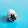
- TRL 7Electronic Drug-delivery Pill
- TRL 8Fiber-optic Biosensor
- TRL 8Haptic Wearable Device
- TRL 9Hyperspectral Camera
- TRL 9Low Earth Orbit (LEO) Satellite
- TRL 7Magnetic Capsule Endoscopy
- TRL 9Magnetic Identity Card
- TRL 8Moss-based Air Filter
- TRL 9Multi-Touch LCD Screen
- TRL 8Quantum Dots (QDs)
- TRL 9Smart LED Light
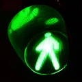
- TRL 8Smart Traffic Lights
- TRL 8Talking Book
- TRL 9Unstructured Supplementary Service Data (USSD)
- TRL 8Wireless Skin Patch Sensor
- TRL 9Wireless Soil Sensor
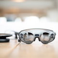
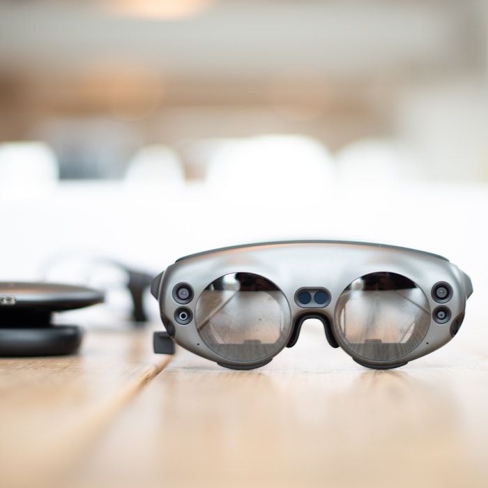
- TRL 8XR Glasses